 AUTOMATIC PHOTOTOOL REGISTRATION UNIT WITH TOP AND BOTTOM LIGHTING CAPABILITY AND PARFOCAL LENS.
The Automatic Phototool Registration Unit sights on two targets that are provided in the panel and aligns two corresponding targets in the artwork film as directed by the vision system. Once alignment of the film is achieved, and any dimensional error between the panel and the artwork split, the operator is signaled to secure the film to the panel. The panel is flipped and the operation is repeated for the second side. The multilayer panel is now ready for imaging.
A great deal of effort has gone into the technology of generating small vias and metalizing them successfully. However, little has been offered in the area of alignment of surface image. Eye alignment of artwork film to extremely small microvias is certain to be tedious and without predictable results. Now there is a system that will ensure the accuracy required with repeatable results.
The application of soldermask to these products has become critical. By providing optical targets in the primary image, with matching targets in the soldermask phototool, the precise alignment of soldermask to surface mount features becomes routine.
All of the technologies available for generating microvias are capable of generating targets suitable for use with the Automatic Phototool Registration Unit.
Some other applications of the Automatic Phototool Registration Unit (APR) in the manufacture of High Density Interconnection Structures:
IR(CO2) lasers are naturally reflected by copper. Therefore it is necessary to etch windows in the copper at the microvia locations to expose the dielectric material below. The APR can automatically register the phototool to the copper clad multilayer panel to image these windows that are subsequently etched. An oversize, defocused beam ablates the dielectric material down to the circuitry below. The optical target, can be either a hole or an etched feature on the signal layer below the surface copper.
UV lasers are capable of ablating copper and FR-4. However, they are non-discriminating and care must be taken to control the energy so as not to damage surrounding areas. For this reason, to remove the dielectric material a small focused beam is used and trepanning forms the microvia through the dielectric. More typically, the beam is directed through windows etched in the copper chemically. Again the APR can register the phototool to create a conformal mask at the microvia locations.
Photoimageable Dielectric formation of microvias requires that a phototool to define the location of the microvias be aligned to the circuitry on the multilayer panel. The APR will align this conformal mask using either an etched feature on the signal layer, or a drilled hole if available from a previous process step. Once the microvias are formed and plated, registration of the surface image to the microvias is the same as above.
Plasma formation of microvias is discriminating. That is, dielectric material is removed from a hole without disrupting or removing the copper at the top or bottom of the hole. Plasma technology also requires a conformal mask to provide etched windows through the surface copper at the microvia locations. As with the Photoimageable Dielectric process, the APR will align the artwork film to provide the windows through the surface copper.
Target configurations for the APR:
Other target types available:
To process other types of targets and to allow for a greater range of target sizes, a parfocal zoom lens assembly is available. The parfocal characteristics of this lens allow the total magnification to be adjusted from 20X to 120X without changing the working distance of the lens. This allows the cameras to be fixed to the machine for better repeatability. This lens set is also telecentric in cases where the total magnification is greater than 52X (1.8X optical). This means that constant perspective and magnification are maintained so that even if the observed object is slightly out of focus, the size of the image, and the ability to measure it accurately are not affected. The parfocal lens assembly can also be combined with fiber optic ring lights (top lighting) to enable the APR to process a wider range of materials.
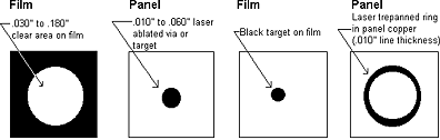
For alignment of conformal masks in Plasma or Photoimageable Dialectric microvia formation, as well as in build up technology, the targets used are very similar to those used in conventional alignment. The difference is that the size of the film targets can range from .010" diameter to .060", while the panel targets can range from .030" to .180". Please note that the panel target should be around three times the diameter of the film target.
Top lighting allows the APR to process opaque panels with laser drilled or ablated targets. Possible target configurations include: A clear area on the film which can be aligned to a laser drilled microvia, and a standard black film target which can be aligned to a laser trepanned ring on the panel copper.
Both of these are useful in aligning outer layer circuitry to laser formed microvias. Home | About Us | Staff | Directions | Products | News | Y2K | Employment | Contact Us
© 1999 Multiline Technology
|
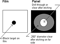 For conventional alignment of outer layer or soldermask phototools, a standard magnification of 40X (1.4X optical, 28.6X electronic) is used. The inner target is usually a .030" diameter black dot on the film. The corresponding outer target is a .090" diameter drilled hole or clear after etching circle in the panel, centered on a .250" diameter area on the far side of the panel which is clear after etching. The target area is lit from underneath (bottom lighting) to ensure sharp contrast for accurate processing.